Specifications of ADCs
ADC Terminology
ADC Registers:
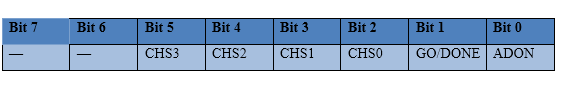
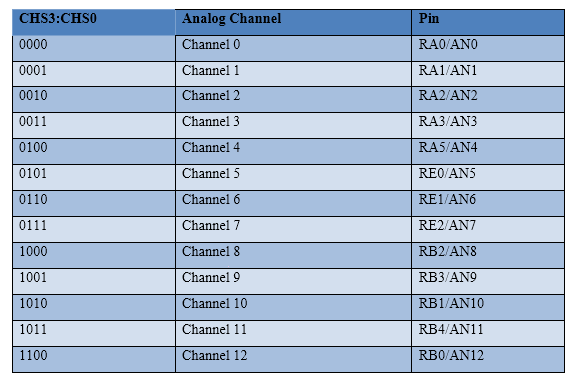
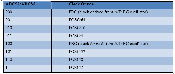
1. ADCON0 (A/D CONTROL REGISTER 0)
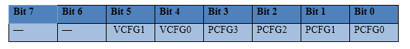
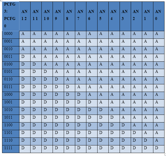
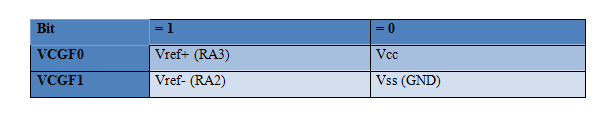
2. ADCON1 (A/D CONTROL REGISTER 1)
3. ADCON2 (A/D CONTROL REGISTER 2)

4. ADRESL & ADRESH:
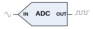
Working with ADC
Programming Steps:
/*  Name     : ADCmain.c
 *  Purpose  : Source code for Inbuild ADC in PIC18F4550.
 *  Author   : Gemicates
 *  Date     : 2017-06-15
 *  Website  : www.gemicates.org
 *  Revision : None
 */

                                    // Program for Inbuild ADC in PIC18F4550
#include<htc.h>                     // Header file for PIC18F4550 series
#define _XTAL_FREQ 12000000         // 12MHz Crystal Frequency for PIC18F4550


void ADC_Init()
{
  ADCON0 = 0x41;                    // ADC Module Turned ON and Clock is selected
  ADCON1 = 0xC0;                    // All pins as Analog Input
}

unsigned int ADC_Read(unsigned char channel)
{
  if(channel > 7)                   // If Invalid channel selected
    return 0;                       // Return 0

  ADCON0 &= 0xC5;                   // Clearing the Channel Selection Bits
  ADCON0 |= channel<<3;             // Setting the required Bits
  __delay_ms(2);                    // Acquisition time to charge hold capacitor
  GO_nDONE = 1;                     // Initializes A/D Conversion
  while(GO_nDONE);                  // Wait for A/D Conversion to complete
  return ((ADRESH<<8)+ADRESL);      // Returns Result
}

void main()                         // main function
{
  unsigned int a;
  TRISB = 0x00;                     // PORTB as output
  TRISC = 0x00;                     // PORTC as output
  TRISA = 0x10;                     // PORTA as input
  ADC_Init();                       // Initializes ADC Module

  do
  {
    a = ADC_Read(0);                // Reading Analog Channel 0
    PORTB = a;                      // Lower 8 bits to PORTB
    PORTC = a>>8;                   // Higher 2 bits to PORTC
    __delay_ms(60);                 // Delay
  }while(1);                        // Infinite Loop
}